Recent advancements in AI have enabled the creation of photonic chip components 500 times smaller, showcasing the potential for enhanced functionality.
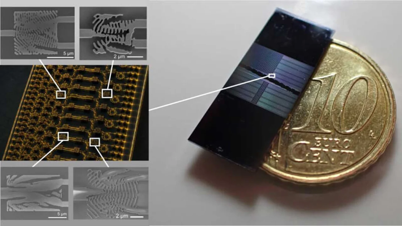
Researchers have achieved a remarkable milestone by dramatically reducing the size of three essential components used in photonic microchips, making them up to 500 times smaller than previous designs. This breakthrough stemmed from an AI algorithm that produced designs considered "beyond human intuition." The resulting compact components open the door to greater on-chip functionality.
Unlike traditional microchips that rely on electrons for processing, photonic microchips harness the power of light (photons). This approach allows them to transmit and process data at significantly higher speeds due to photons traveling at the speed of light. Additionally, photonic chips support higher bandwidth by utilizing different wavelengths for distinct data streams, resulting in lower energy loss compared to electronic counterparts.
These photonic chips find applications in areas where rapid data transmission is critical, including fiber-optic communications, data centers, autonomous vehicle lidar systems, and quantum computing.
Light propagation on photonic chips is directed through channels known as waveguides, rather than traditional metal wiring. Each chip is equipped with essential components like wavelength splitters, spatial mode sorters, and mirrors, all designed to manipulate light within a remarkably small footprint.
The study, published on May 28 in the journal Nature Communications, confirms that the newly created space on these chips has the potential to "unlock new functionalities," as noted by the researchers. This work illustrates how AI can facilitate the design of complex components that are not only novel but also feasible for manufacturing.
AI's Reverse Engineering of Component Designs
The research team utilized an AI algorithm by first specifying the desired behaviors of light within the components while adhering to manufacturing constraints, such as limitations on the curvature of nanostructures. The AI then employed a reverse engineering approach, iteratively testing and refining various designs to achieve optimal performance.
Toby Bi, the lead author of the study and a researcher at the Max Planck Institute for the Science of Light, expressed excitement over the AI's capabilities. "Inverse design lets us define what we want light to do, and the optimization finds a structure that does it, often one no human would have drawn," he stated in a statement. The AI's framework allows for multiple functionalities on the same chip, organizing light by wavelength and spatial mode while serving as mirrors for on-chip optical cavities.

Traditionally, photonic chip components have been crafted through manual engineering, a process that limits creativity and adds time. The AI-driven design approach allows for exploration beyond conventional geometries, accelerating the development of next-generation devices.
In enhancing their components, the team chose to fabricate them from thick silicon nitride, measuring approximately 400 to 800 nanometers thick, as opposed to the standard 150 to 400 nanometers. This material choice minimizes light wastage while ensuring better confinement of wavelengths.
The mirrors developed in this research, measuring about 11 μm, are capable of reflecting 98.5% of incoming light while effectively blocking unwanted patterns. In a pair configuration, light can bounce between the mirrors over a hundred times before escaping, emphasizing the low-loss characteristics of the silicon nitride.
Integrating AI-Designed Chips into Real-World Applications
Despite successfully demonstrating the individual components, the team has yet to combine them into a fully integrated optical circuit. This integration step will be critical for developing functional photonic chips that leverage the increased component density achieved through these novel designs.
- Scientists figured out how to shrink huge ultrafast lasers so they fit on a tiny chip — the 'holy grail' of the field
- Breakthrough in experimental light-powered quantum computers could mean scaling them up is now far more viable
- New wonder material designed by AI is as light as foam but as strong as steel
The research provides promising insights into the feasibility of compact, robust photonic components that can be fabricated en masse. "These results demonstrate the feasibility of compact, fabrication-error-robust, customized photonic components and pave the way for scalable, high-performance integration in silicon nitride-based photonic systems," the researchers concluded in their study.
As AI increasingly integrates into semiconductor design and fabrication, engineers have started to witness substantial improvements in efficiency, shortening design cycles from weeks to hours, and significantly cutting costs. Notably, models like Google’s AlphaChip have produced "superhuman" chip designs that are now being used in the company's production of AI chips, showcasing the transformative potential of AI in this arena.
Discussion
Sign in to join the discussion.