A newly developed transistor can withstand temperatures over 1,110°F, making it a potential game changer for future Venus probes and high-stress applications.

Researchers in Japan have created a transistor capable of functioning at an astounding 1,110 degrees Fahrenheit (600 degrees Celsius). This technology may play a crucial role in future exploration missions to Venus, where surface temperatures can soar to 860°F (460°C) due to its dense carbon dioxide atmosphere.
Transistors are integral to modern electronics, managing electrical current in devices ranging from smartphones to deep-space probes. The new device is a junction field-effect transistor (JFET), which alters its conductivity through electrical fields, marking a departure from conventional transistors found in consumer technology.
Typically, JFETs are utilized in specialized contexts due to the challenges they present in miniaturization compared to the prevalent metal-oxide-semiconductor field-effect transistors (MOSFETs). However, they provide less noise interference since their operation doesn't depend on an oxide layer.
The findings related to this new high-temperature transistor were published on August 17 in APL Electronic Devices.
Challenges of Heat Resistance
Since the early 2000s, silicon carbide (SiC) JFETs have been recognized for their potential in high-temperature applications, particularly for missions geared towards Venus. Historical landers have faced severe limitations; for instance, the Soviet Venera 13 spacecraft managed to operate for just over two hours due to silicon-based electronics' vulnerability to extreme conditions.
The research team emphasized that “past landers have been limited to only a few hours by silicon-based electronics.” Integrated circuits made from SiC are appealing for their robustness in extreme environments such as space exploration, geothermal drilling, and aerospace functions that conventional silicon circuits cannot reliably withstand.
Previous SiC-JFET designs encountered two significant hurdles: limited controllability and excessive leakage currents. These issues stem from how the SiC substrate is doped with various atoms—this affects both the gate region, where the electrical field is generated, and the channel region, where the current flows.
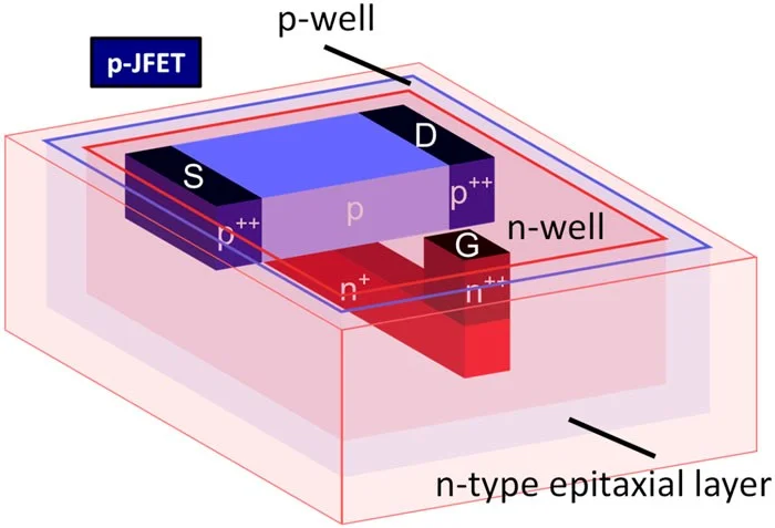
In crystalline materials like SiC, dopant atoms can sometimes penetrate deeper than intended, affecting electrical properties at elevated temperatures. This phenomenon can increase the field voltage needed to activate the channel and complicates the transistor's control. Researchers noted that this issue could shift conventional JFET voltage thresholds by over 2 volts.
Moreover, above temperatures of 660°F (350°C), SiC can become less electrically resistive, allowing unintended current flow even when the transistor is in the off state, leading to erroneous signals and higher energy consumption.
While current high-performance JFETs struggle to maintain functionality at temperatures over 930°F (500°C), the Kyoto team posited that these persistent issues may arise from misapplying silicon-based principles to SiC technology. First author Mitsuaki Kaneko, an associate professor of engineering at Kyoto University, remarked that the research community has often approached SiC with outdated methodologies.
Design Innovations
The new SiC-JFET design from the research team addresses previous challenges directly. By employing a bottom-gate configuration—where the gate exists beneath the conducting channel—the researchers have enhanced controllability. The gate region is heavily doped, insulating it from the impact of deeper-penetrating dopant atoms, thus stabilizing the threshold voltage even under intense heat.
Additionally, the design incorporates semiconductor regions, referred to as “wells,” which create barriers to current flow. These barriers ensure that even if the SiC becomes more conductive at high temperatures, current cannot bypass the channel when switched off.

The researchers assessed the new JFET's current-switching capability and compared its actual threshold voltage to theoretical expectations across temperatures from room temperature up to 1,110°F (600°C). The outcomes indicated that the devices maintained stable operations above 873 K (1,110°F), indicating significant promise for high-temperature SiC applications. Remarkably, at around 750°F (400°C), they found the error in threshold voltage to be under 0.1 V.
This transistor has implications far beyond Venus probes; it could also enhance designs in jet engines, where current components require extensive thermal protection systems. The potential for integration into complex circuits and further testing is on the horizon, setting the stage for robust applications in extreme conditions.
Given past successes, such as NASA's demonstration of SiC-JFETs' reliability under high temperatures and stress, there’s optimistic anticipation for future applications in both aerospace and planetary exploration.
Discussion
Sign in to join the discussion.